Introduction
Below is a collection of notes regarding the Binary Decoder and the Power Board. This covers the operating principles of these boards, how I came to the decisions on parts, and other general guidelines on designing your own boards.
Making the Special Edition Board
|
|
Making the Special Edition PCBs is quite tricky. I cover the entirety of both the top and bottom of the board with a copper pour. In a normal PCB, this makes for a better, more consistent looking board. However, copper pours on a clear solder mask lead to an ugly off-copper colored board. Therefore, I had to replace the pours with traces. While this is not too hard in and of itself, the extra challenge is that I could not move any of the parts (otherwise the instructions may become confusing, the stencils would no longer align, etc.).
You can see on the left all the additional traces that are required to make the Special Edition board work.
|
Choosing a Microcontroller
|
For through-hole projects, choosing the microcontroller is easy. For big stuff, the 328P is ubiquitous, and for smaller stuff, the AtTiny 25/45/85 are perfect. When it comes to SMD, it gets a bit more complex though.
When choosing a microcontroller, there are a few key things I look for. The first and most important thing is open ease of use. Anything I integrate into an educational kit should work seamlessly with Arduino, and not require and awkward programming modes or adapters.
The second thing is availability. I like to find microcontrollers that can be commonly purchased in single-item quantities from manufacturers. This not only makes my life easier for prototyping, but it also means that if you like the microcontroller from the kit and want to try it in your own project, it is easy to just buy the same part for yourself.
The third aspect is expandability. I try to have it so that the firmware for a project only takes up about 30 to 50% of the program memory. That way, users can create their own firmware and upload it to the board that either has more features or is not as optimized without concerns.
|
The fourth consideration is solderability. Many microcontrollers come in the more space-efficient QFP package, such as the SMD version of the 328P. The issue is that QFP packages have pins on all 4 sides, so when lining up the part, you have 2 dimensions of movement to get right. So many times when I started soldering, I'd get the first pins or the first 2 sides lined up beautifully, only to look at the other 2 sides and see that it is a hot mess. Only having 1 dimension to worry about with an SOIC IC makes life a lot easier.
How many ICs is too many ICs?
|
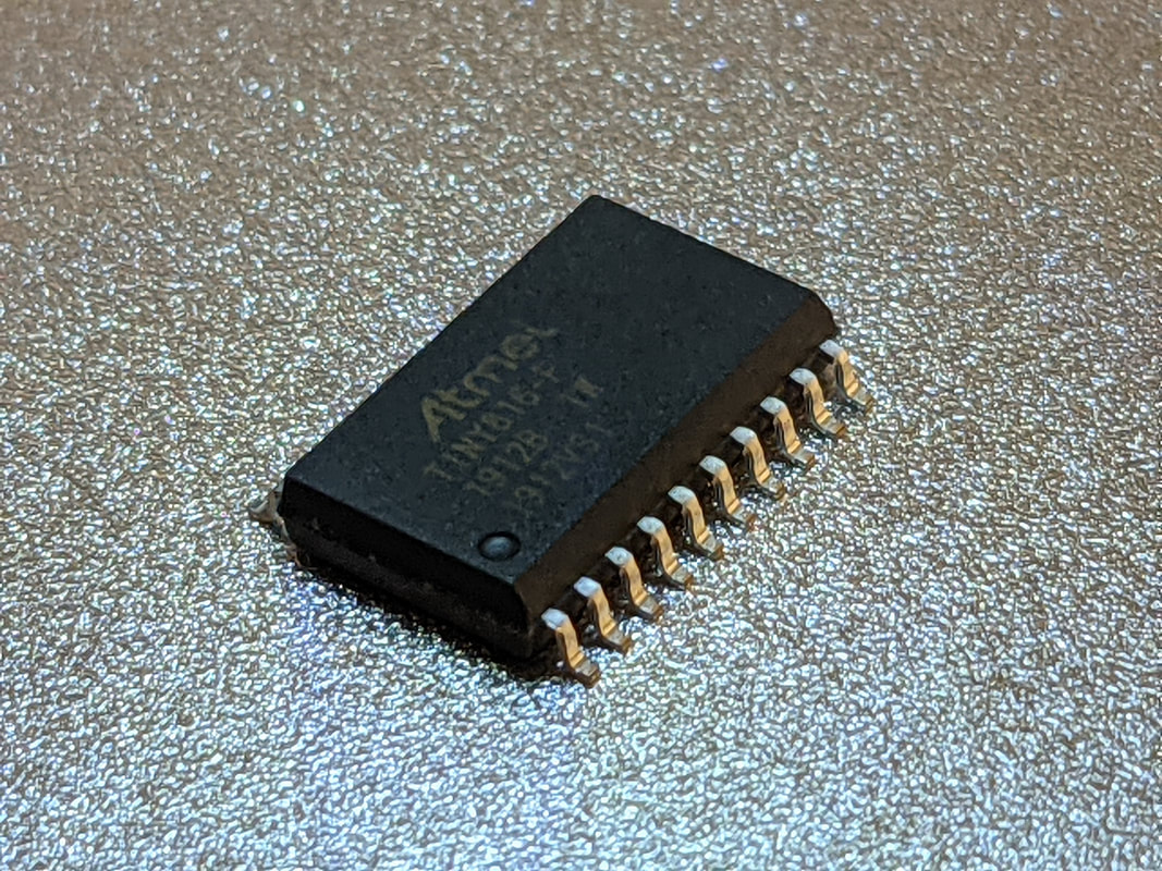
The Binary Decoder has gone through 8 revisions before getting to this point. Looking at the original design (to the left), it is clear that a lot of stuff has stayed relatively the same. The biggest difference you can see is that there are 3 ICs instead of the 2 on the current kit. The MCP23017 is still there (it is a super useful chip that I love to use), but the AtTiny 816/1616 was originally an AtTiny 1614, a chip with much less IO than the 1616. To compensate for the lack of I/O, a third IC, a CD4026, was used to drive the LEDs.
The original idea was that each of the 3 ICs could be used to learn a different soldering technique for SOIC packages. However, many advanced SOIC soldering techniques (like drag soldering) proved too complex in early testing and led to too many bridges and short-circuits. On top of that, the CD4026 was finicky to work with, would have limited the number of LED colors I could use (many colors are only available as common anode or common cathode, not as both), was hard to identify (no writing, no dimple on pin 1, etc.) and was the same size as the AtTiny 1614, leading to fears that someone may accidentally switch their positions and destroy the Binary Decoder.
|
With all of those in consideration, there was another reason to switch from the 1614 to the 1616; body size. The MCP23017 is considered a "wide" SOIC, whereas the 1614 is more the standard width. However, I found that the wider SOIC package was easier to hold and align, making it easier for people new to soldering. So, I was able to find the 1616 in a wide body SOIC, and it was much easier to solder.
Now on the opposite end of the spectrum is the question of why I used 2 ICs, rather than just 1 larger one. There are tons of microcontrollers with more than enough pins to run everything, and it would have led to simpler code and far more responsive LEDs and buttons (not that anyone really cares about the 1 millisecond delay anyway, but still), not to mention ditching the I/O expander likely would have saved a bit of money. In addition to what I mentioned above about microcontroller selection, there are 2 big benefits I see to using 2 chips rather than 1. The first is creative freedom. If there was 1 massive IC running the entire board, It'd likely have to go dead center to reach everything. This would have led to a larger board and a more awkward layout. By splitting the board into 2 sections, each going to their own IC, I can condense things and move them around a lot more. The second is ease of soldering. Let's say you put the 1616 onto the board slightly askew. The first pin lines up perfectly, maybe the second and third one too. But as you work down the chip, that skew is going to be amplified. By the time you get to the 10th pin, you may barely be on the pad! Now imagine how much more precise you'd have to be if it was a 30 pin IC. By having it be 2 separate chips, you basically have a checkpoint in the middle to re-align and compensate for errors.
Who uses 1206 these days?
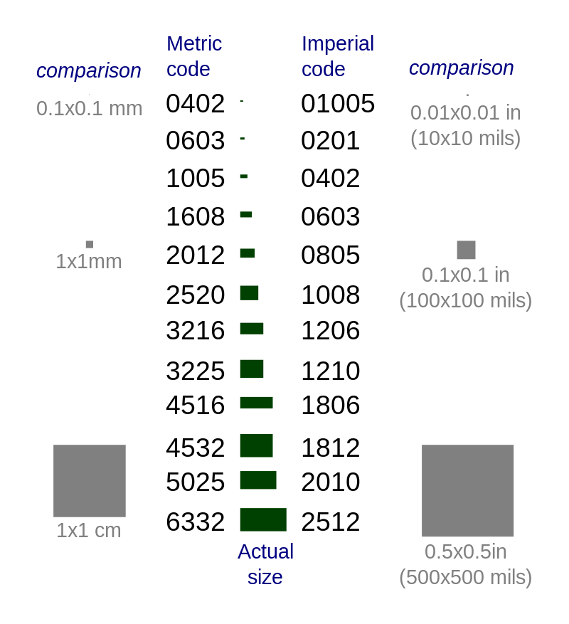
Source: Wikipedia
|
Note: I use the more common imperial code for components, but the chart to the left also has the somewhat confusing metric code, which occasionally has identical names to the imperial code for different parts.
While developing the Binary Decoder, I gave a lot of thought to part sizing. 1206 is the largest common size you'll find for most components, but it is rare to see in actual use today. The only place I really see 1206s anymore is for capacitors that, by the laws of physics, cannot be made any smaller.
On the one hand, the argument for 1206s, especially in a board targeted at those new to SMD, is clear. The parts are larger, so you have a larger area to solder and lower tolerances if you do mess it up. The parts are big enough you can see them with the naked eye and move them with your fingers.
On the other hand, all the arguments about tolerancing and spacing go out the window when you realize the pitch on an IC is closer to an 0805 or 0603 component, so you already need to be good enough to solder smaller pitches. In addition, these smaller parts are more readily available, cheaper, and more commonly seen in real products.
Ultimately I opted for 1206 to keep the learning curve gentle, but to anyone reading this who does want to get more into SMD, I'd highly recommend picking up a kit that uses 0805s or 0603s after this.
|
USB-C Sucks
|
As a consumer, I love USB-C. A study, reversible connector, with higher current limit, and universal compatibility with most other modern products.
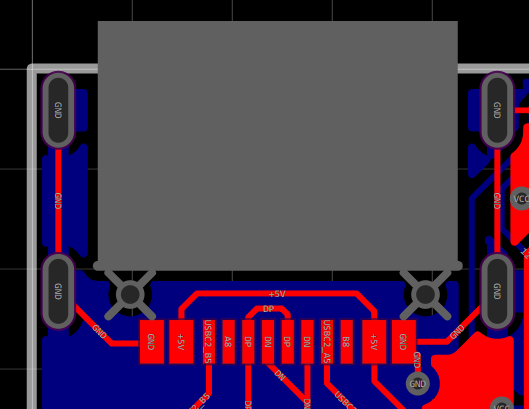
As someone who designs soldering kits, I hate USB-C. For comparison, look at a Micro-USB port. In the same space as a USB-C port, it needs 4 (sometimes 5) pins to get not only power, but data as well. These pins also tend to be smaller, allowing for more solder mask between pins, reducing the risk of bridging. By contrast, a USB-C port needs 6 pins and 2 resistors just to get 5 volt power. If you wanted USB 1.1-speed data in there, you'll need to add an additional 6 pins. This takes the USB-C connector well into the realm of non-solderable by hand, so you'll have to resort to an assembly service or use a stencil and hot plate. To top it all off, USB-C ports are also extremely expensive, due to how complex they are. An average-quality Micro USB port is usually around $0.02-$0.05, depending on how many you buy. The absolute cheapest power-only USB-C port I've ever found is $0.55 in single-piece quantities, and it is rare to see a data USB-C port from a reliable vendor under $1.
|
Designing the Power Board
|
|
When I ran the Kickstarter for the Binary Decoder, some educators reached out to me and asked about the feasibility of making the decoder work independent of a power source. This'd make it a lot more useful for use in a classroom environment. So, I set about designing an add-on that can strap on and power the board from a battery.
In hindsight, there are 2 much simpler Power Boards I could have designed. The first and simplest one is just a board with 3 AA batteries, right into Binary Decoder. The Watchdog on the AtTiny will allow it to operate down to about 3.6 volts, well below the voltage of 3 even near-depleted AA batteries. The second simpler design I could have opted for was an LDO and a 9 volt battery. This would have made clean, precise 5 volt power with just 3-4 components.
Instead, I opted for a 2 AA battery boost converter. The advantage of this over the other options is that it'll be smaller/lighter, and provide more learning opportunities. The challenge then came to finding a suitable boost converter IC.
|
For most of my personal projects, I like to use Texas Instruments buck/boost converters. They are super easy to use and provide tons of added benefits, but have some serious drawbacks. The first is that they are generally 8 times more expensive than the solution I opted for. The second, and arguably worse, issue with them is that they generally come in a VQFN package. This means that the part is a tiny rectangle, with pins on all 4 sides with less than 0.1mm between each other. To make soldering even harder there isn't actually a pin there, it is just a tiny copper edge on the part. It is up to you to form the solder into a blob that connects from the side of the part to the pad.
So those were out of the running. On the other extreme end of the spectrum, there are tons of inexpensive and powerful "boost controller" ICs. They are commonly found embedded in real products. The biggest difference between a controller and a converter IC is that the controller requires significantly more external components to get everything working properly, and generally offers fewer protections. For a real product the savings makes it worthwhile, it can reduce the cost of your boost converter by up to 90%. However when you are selling something to solder by hand, it is not ideal since it requires a lot of very specific parts placed very particularly, and messing up or missing one part can lead to the whole thing melting.
I ended up setting on a massively overkill boost converter. It is rated to handle a continuous 2 amps, whereas the Binary Decoder usually draws only about 100mA. The big deciding factor was all the baked-in safety features. In testing, the IC handed overvoltage, undervoltage, overcurrent, short-circuit, and dozens of other terrible conditions. Once the issue was removed, the board powered back on immediately with 0 issues. The compromise made to use this IC is that it is not generally meant to be used with AA batteries. Modern AA batteries have a nominal voltage of 1.5 volts, so 2 in series should produce 3 volts. The boost converter generally works down to 2.5 volts, and below that the output voltage will sag and the inductor may start to whine, due to the extra load.